FC CSP substrate (Computers - Hardware)

Item ID 2497135 in Category: Computers - Hardware
FC CSP substrate | |
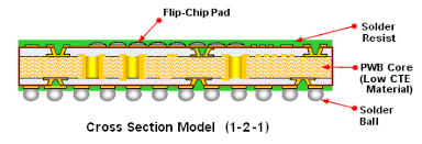
Flip chip does not depend on the wire bonding as a means of interconnection but it uses solder or bumps such as copper pillar. This means that the I/O pads can be placed at any section of the surface of the chip and therefore the chip size can be reduced with an appropriate circuitry path. This is attributed to the fact that the absence of a bonding wire contributes to the minimization of signal inductance. Contact Info:- High Quality PCB Co., Limited Office: Shajing Town, Baoan District, Shenzhen, Guangdong 518000, China Plant 1 address: Building 5-6, Fu Qiao 3rd Industrial Zone, Bao' an, Shenzhen, Guangdong, China Plant 2 address: Zhuhai, Guangdong, China Plant 3 address: Dongguan, Guangdong, China TEL: +86-755-23724206 WhatsApp: +86-189 2381 2997 Skype: shawnwang2006 Email: sales@efpcb.com  | |
| Target State: All States Target City : Shenzhen Last Update : 08 October 2024 4:50 PM Number of Views: 116 | Item Owner : Shawn Wang Contact Email: Contact Phone: +86-755-23724206 |
| Friendly reminder: Click here to read some tips. | |
© 2025 AUNetAds.com
USNetAds.com | GetJob.us | CANetAds.com | UKAdsList.com | INNetAds.com | CNNetAds.com | Hot-Web-Ads.com | USAOnlineClassifieds.com
2025-04-20 (0.466 sec)